DIY VNA calibration standards
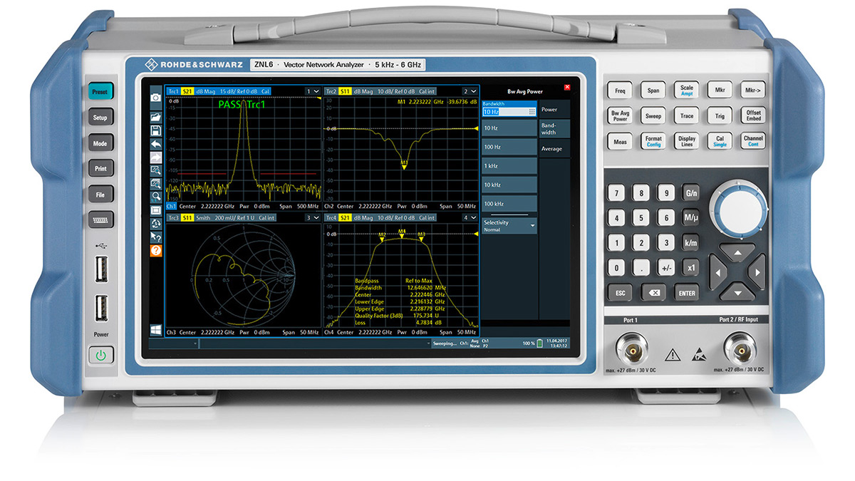
The vector network analyzer (VNA) is one of the most formidable pieces of test equipment you’ll encounter in a general-purpose electronics lab environment. Highly sensitive (variation in the torque applied to connectors can show up in measurements) and extremely expensive (more than oscilloscopes), VNAs also require calibration before each use. Without a characterized calibration kit, measurements from a VNA are unreliable.
A typical calibration kit consists of standards for open, short, and matched loads (OSL) on a single port, and a through-connection for connecting two ports. At radio and microwave frequencies, the physical realization of a simple open or short circuit becomes complicated, because the effects of stray capacitance and inductance, and electrical length in physical objects can no longer be ignored. An open circuit actually has some fringing capacitance, a short circuit has some inductance, and a load that reads a perfect 50 Ω on a multimeter could be inductive or capacitive at higher frequencies.
Commercial calibration kits can cost thousands of dollars, and are precisely machined and individually measured against an even more expensive calibration standard. Where does the ultimate source of truth about calibration come from? At the highest levels of metrology, calibration is verified against precision air-dielectric transmission lines with dimensions accurate to 1/10000 of an inch, which must be handled with gloves to avoid contamination. It eventually comes down to geometry, and what Maxwell’s equations tell us about how electromagnetic waves will propagate through that geometry.
What if I took a geometric modeling approach to designing homebrew calibration standards? My needs are pretty modest: I have a combination spectrum analyzer/single-port VNA that can measure up to 3 GHz. Surface-mount SMA connectors are cheap, and could be terminated to produce a OSL kit. Their dimensional accuracy is not as good as an airline, but better than you can measure on a typical set of calipers. Until recently, getting numerical solutions to Maxwell’s equations with arbitrary 3D geometry (known as full-wave electromagnetic simulation) was out-of-reach of amateurs. Licenses for software like Ansys HFSS cost tens of thousands per seat. openEMS, first developed in 2015, is one of the first free and open-source 3D EM field solvers. It is not the easiest thing to learn, since geometry is created by Matlab code, and is limited to combinations of geometric primitives like boxes, cylinders, and spheres. EM field solvers are also notorious for their garbage-in-garbage-out behavior; if the geometry is slightly off, or is discretized in a bad way, the simulation will still run and give you completely crazy results. Thankfully, openEMS also provides tools to visualize the discretized geometry pre-simulation, and wave propagation during simluation to catch errors.
Physical construction
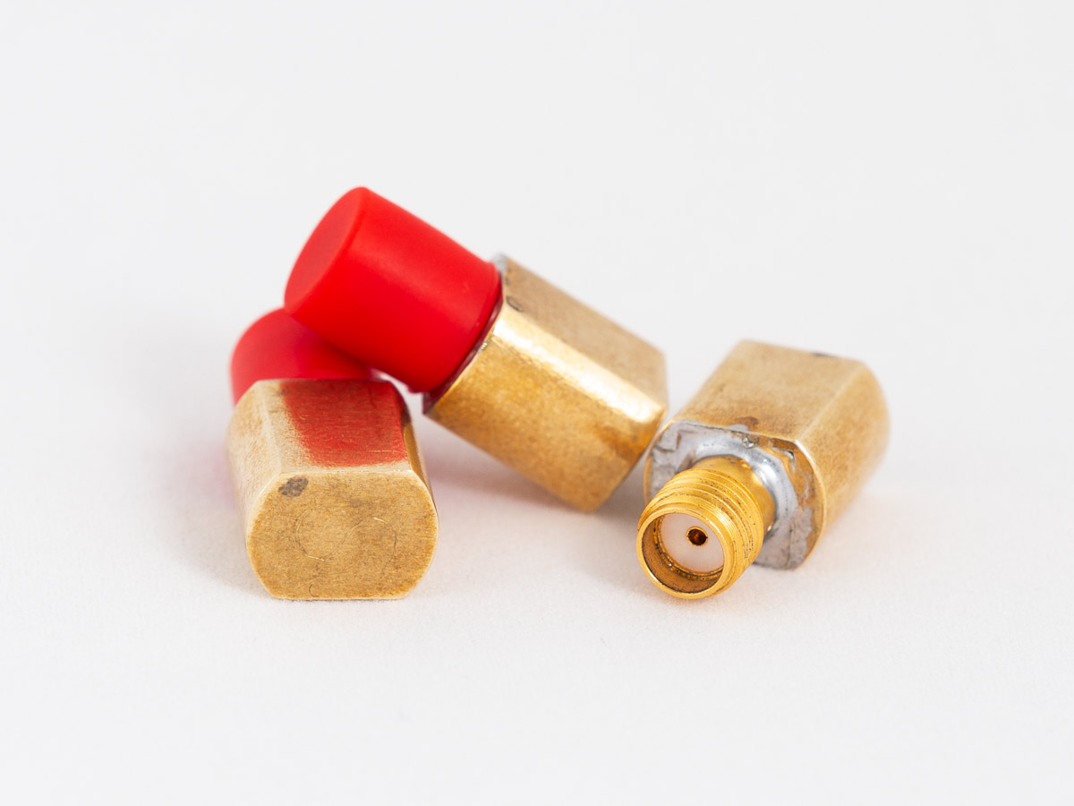
To build my own standards, I started with the 32K10A-40ML5, a high-quality surface-mount SMA connector from Rosenberger. The datasheet has dimensioned drawings and guarantees a VSWR figure up to 12.4 GHz. I designed a brass fitting that would enclose and shield the termination, and provide flats to hold the standard with a 5/16” wrench, which is the same size used to tighten the SMA hex nut. I had three of these fittings printed from brass by Shapeways.
The standards were constructed as follows:
- Open: the SMA connector was mounted unmodified in the fitting.
- Short: a piece of 30-gauge copper sheet was cut to fit the base of the connector, and solder was reflowed to short the center pad to the housing.
- Load: a pair of precision 0.1% thin-film 100 Ω resistors was soldered in place at the end of the connector. 0805 is the right size; any smaller and it won’t bridge the gap across the dielectric, and soldering becomes tricky and not very repeatable. The best RF resistors are not available in this size, but they don’t provide any advantage below 3 GHz. The resistive film is on the top of the resistor, and I had the choice of soldering them face up or face down. Face down would have less inductance but would create a stub at the center pad. I decided to leave them face up.
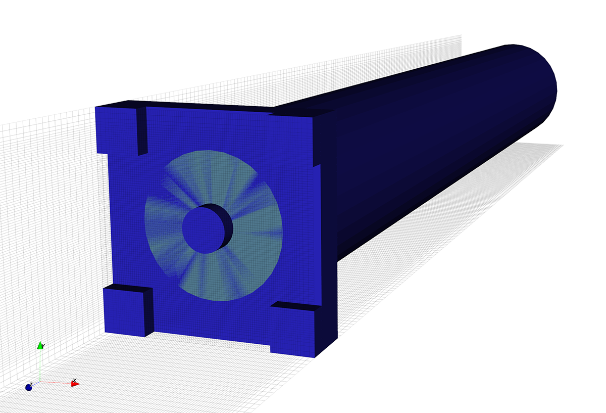
Modeling and simulation
To model the standards for simulation, I created a 3D model of the connector geometry and coaxial feedline. The effect of the brass enclosure was modeled in openEMS by using a perfect electrical conductor (PEC) as the boundary condition around the termination.
- Open: the unmodified connector geometry and boundary condition was used.
- Short: the copper shorting pad was modeled as a conducting sheet of metal at the end of the connector.
- Load: each of the 0805 resistors was modeled as a box of alumina dielectric for the body, a U-shaped assembly of metal planar elements for the terminations, and an ideal resistive material across the top that would amount to 100 Ω.
After I had the geometry and materials modeled, I ran the simulations. Dozens of times. I tried testing adjustments to the mesh, different amounts of space between the boundary layer, trying to find the sweet spot between simulation speed and stability. Every change offered some tradeoffs, but the quality of the results began to stabilize. The output of the simulation was a table of frequency and complex impedance values in plain text format that is uploaded to the VNA and used during the calibration procedure.
Verification and discussion
To check my work, a member of the EEVBlog forum was kind enough to characterize my standards on a monster of a VNA, the 26.5 GHz Keysight N5222B, as well as a 8714ES. It’s not everyday you get to measure your homemade creations with a $100K piece of equipment!
To evaluate the simulation results, I plotted the magnitude and phase of

Characterized on the N5222B, the open standard shows very close agreement to its simulated performance. The difference in the phase response amounts to about 0.35mm difference in electrical length. There is some loss that begins to increase after 1 GHz, but it is less than 0.1 dB at 3 GHz.

The short standard shows a little more deviation from its predicted result. This is a discrepancy of about 2mm in electrical length, which is just over 10% of the predicted length, but this is still a good result.


The load standard follows the predicted return loss, but the phase response shows an unexpected difference. The simulation predicted a capacitive load, while the N5222B measured something inductive over most of the frequency range. When I examined the results obtained from the 8714ES, the measured phase response is a closer match. Without remeasuring, it’s hard to say what happened here. Since the standard presents a nearly exact 50 Ω load, any inconsistency in laboratory procedure can show up as a large error in the phase response.
The confirmation of the simulation results was satsifying — and a relief, given the fickle nature of electromagnetic simulators. For applications below 3 GHz, I wouldn’t hesistate to save money and use DIY standards carefully constructed from off-the-shelf connectors along with the simulated s-parameter data for VNA calibration.
Further work
In considering how to improve the construction of standards using off-the-shelf components, I looked at solderless compression-mount connectors. These are high-end connectors that are designed to be fastened to a PCB with screws and make direct contact to traces on the board. Since they lack solder pads, they don’t have elements that can act as unwanted stubs or inductance for the open and short standards. For the load standard, the connector could mount to a small PCB that terminates the transmission line using microwave-grade resistors. I expect these construction techniques could extend the usable frequency range of the standards well above 10 GHz. Realizing these improvements would need further simulation work and different housings to fit the connectors.
References
All simulation and data files for reproducing these results are available on Github: vna-standards.