Nixie Tube Power Supply
This article is an abridged summary of my project logs from April 2020 on hackaday.io.
The goal of this project was to build a flyback converter to boost common voltages of 5–12 V to 170 V for powering Nixie tubes. I’ve previous built converters using a boost topology, and a much earlier attempt to power Nixie tubes from USB was my entry point into studying electronics. I designed and tested this converter during April and May of 2020 as a pandemic lockdown project. For this design, I wanted to try a flyback topology and also use a newer controller chip from TI. I built the prototypes as evaluation boards to characterize the converter performance on its own.
Theory of operation
The flyback converter finds many applications in DC-DC and rectifier designs. It can step voltage up or down, and can be built with and without isolation, and can usually be realized with low parts count [1, pp. 194–198]. This is the basic schematic for the flyback converter (the magnetizing inductance

When the switch

When the switch

When a switching converter is operated at low frequencies or light loads, the inductor current may drop to zero in the switch-off state. Because the diode is a unidirectional switch, the inductor current cannot go negative, and the converter operates in the discontinuous conduction mode (DCM). In DCM, the variation in inductor current is no longer small compared to the average value, and more careful analysis of converter dynamics is required. During the evaluation of this project, I found that the transformer would not operate efficiently at frequencies that support continuous conduction mode (CCM).
If the load
The converter’s steady state behavior can be formally analyzed through state-space averaging [1, pp. 251–271] [2]. In this technique, the state-space representation of the converter circuit is averaged over the period of a switching cycle. The formal application of state-space averaging using matrices lends itself well to computer evaluation to simultaneously solve for all DC characteristics of the circuit. The state space equations can also be differentiated to obtain a small-signal AC model, which is used for understanding how feedback can regulate the converter’s output.
A Nixie Tube Power Supply
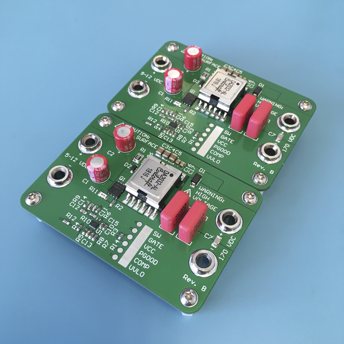
A Nixie tube is a cold-cathode glow discharge tube that was popular during the mid-20th century for numerical readout displays. They require a high striking voltage (nominally 170 V) to start that makes them hard to interface with modern low-power electronics. Since they do not need much current, one way to get this voltage is to boost it from a lower level supply using a switching DC-DC converter. For this project, I designed a standalone converter board for testing and optimizing a design I could later integrate into a larger project. I wanted to follow “evaluation board style,” which to me means:
- low-density design where there’s plenty of room to probe and rework parts
- preference for larger component packages that are easier to rework, minimum 0603 for passives
- lots of test points with nearby ground references for accurate probing
- banana jack terminals for fast, positive connections to meters and power supplies
- screw holes and standoffs at the corners to keep the board stationary while attaching probes
Parts selection
I started the design process with selecting the critical components for the power stage: the controller, switching transistor, transformer, and diode. One reason I took up this project was to design something with the LM5155, a new boost/flyback/SEPIC controller that TI introduced in 2019. It offers a number of improvements over the LM3478 controller I was previously familiar with, such as an adjustable soft-start, wide switching frequency, and very low voltage operation [3].
Flyback transformers are specifically designed with a gapped core so they can store and transfer energy. There are only a handful of commercial off-the-shelf flyback transformers that have a high turns ratio (
One advantage of the flyback topology is the switch doesn’t need to block the full output voltage, so a lower-voltage, higher-performance part can be used. For a switching MOSFET, high performance means lower on-resistance
While the MOSFET gets off with light duty, the diode is reversed biased with a voltage of
Design and simulation
The switching frequency was chosen by working backwards from the peak inductor current rating. When my initial CCM design suffered from poor efficiency, I reduced the switching frequency to operate the converter in DCM. I settled on a frequency of 120 kHz to stay below the 3 A saturation rating of the DA2032.
The input and output capacitors were chosen to keep the input and output voltage ripple to about 100 mV and 1 V, respectively. Nixie tubes were often run from crudely rectified AC power, and they are tolerant of significant voltage ripple. The remainder of the parts selection was dictated by the LM5155 datasheet. While flyback converters can be designed with output isolation by using optoisolators, these parts draw significant current and the design is only rated to 30 mA, so I used a nonisolated topology for simplicity and higher efficiency.
The soft-start of the LM5155 is adjustable with an external capacitor. Some later simulations of my design showed a longer startup time keeps the converter out of CCM during the startup transient, so the startup ramp time was set to 5 ms.
One of the many tricky parts of building switching power converters is designing the compensation network for the feedback loop. Many practical books and guides do not provide detailed advice on the subject and more or less suggest a trial-and-error approach. It’s rare that a switching converter will flatly not work due to a carelessly-designed compensation network, but a poorly tuned feedback loop can lead to slow or oscillating behavior in response to changes to the input voltage or load impedance. Instead of this purely empirical approach, I derived an analytical model of the feedback loop transfer function, which informed better choices of the compensation network. A first-order model of the DCM flyback’s feedback loop is a single-pole system, with identical gain and pole frequency to a buck-boost converter. I combined this model with other elements of the LM5155’s feedback loop in a Python script that selects the compensation network components to meet a target crossover frequency of 1/10th the switching frequency and a phase margin of 60°.
In my initial design process, I ran several circuit simulations in SPICE after chosing parts and design parameters. The simulations showed the design met the output voltage requirement and demonstrated good stability, but also revealed the need for a primary-side snubber to protect the switch from voltage spikes above its 40 V rating. I incorporated a RCD snubber based on an application note from Fairchild Semiconductor [4].
Layout
The LM5155 datasheet provides several helpful layout guidelines and examples, and the engineering team at TI also produced three evaluation boards (in boost, isolated flyback, and SEPIC topologies) that demonstrate good layout. Since PCB layout can be critical for a working switching converter, I was more than happy to copy a layout that works. As the flyback power stage is the only thing on the board, I also used a two-layer layout like the examples and commercial evaluation boards. Without a tightly-coupled and continuous ground plane in a four-layer design, careful attention must be paid to current paths to reduce stray inductance. I went through two board revisions in evaluating this converter; one of the motivations in doing rev. B was to improve the primary side current return path. These improvements reduced the input voltage ripple by 50%.
I wanted to characterize all aspects of the converter, so I built the prototype boards with evaluation in mind. The board has a row of test points to make probing easier. For characterizing the feedback loop, I added a small series resistor before the feedback network as a signal injection point, away from other components to make it easy to rework and remove a connection.
Performance and evaluation
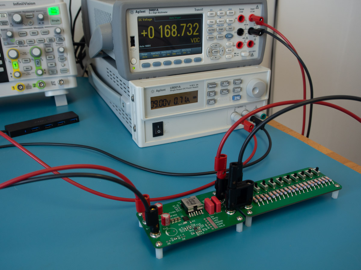
Using a bench power supply, multimeter, and oscilloscope, I characterized the converter’s performance. The typical output voltage is 168 V with a 1.4 V (peak-to-peak) ripple at full load (30 mA). With the rev. B design, the input ripple is just below 100 mV (p-p). Additional capacitance can further reduce the output ripple, but I didn’t see a need since Nixie tubes can tolerate significant ripple. Measurements of the switch node and secondary voltage showed the voltages remained within limits for the MOSFET, but a 600 V diode would be needed. The secondary-side voltage spikes were not amenable to snubbing without paying a high cost in efficiency.
For testing the feedback loop performance, I built an injection transformer based on a design from EEVBlog forum members. The transformer was constructed by winding twisted pair wire around a high-permeability core. This allows a low-level signal to be injected with isolation over a wide range of frequencies. The technique I used for measuring the feedback loop is documented in a Texas Instruments application note [5]. After making connections to my oscilloscope’s function generator and inputs, I used its frequency response program to generate a Bode plot of the feedback loop response. The dynamic range using an oscilloscope is not great; once the difference between channels is over 30 dB, the noise becomes too much to be useful, but the result is still useful near the crossover region. The script I used set a target crossover frequency and phase margin of 12 kHz and 60°, and the measured values were 12 kHz and 50°.
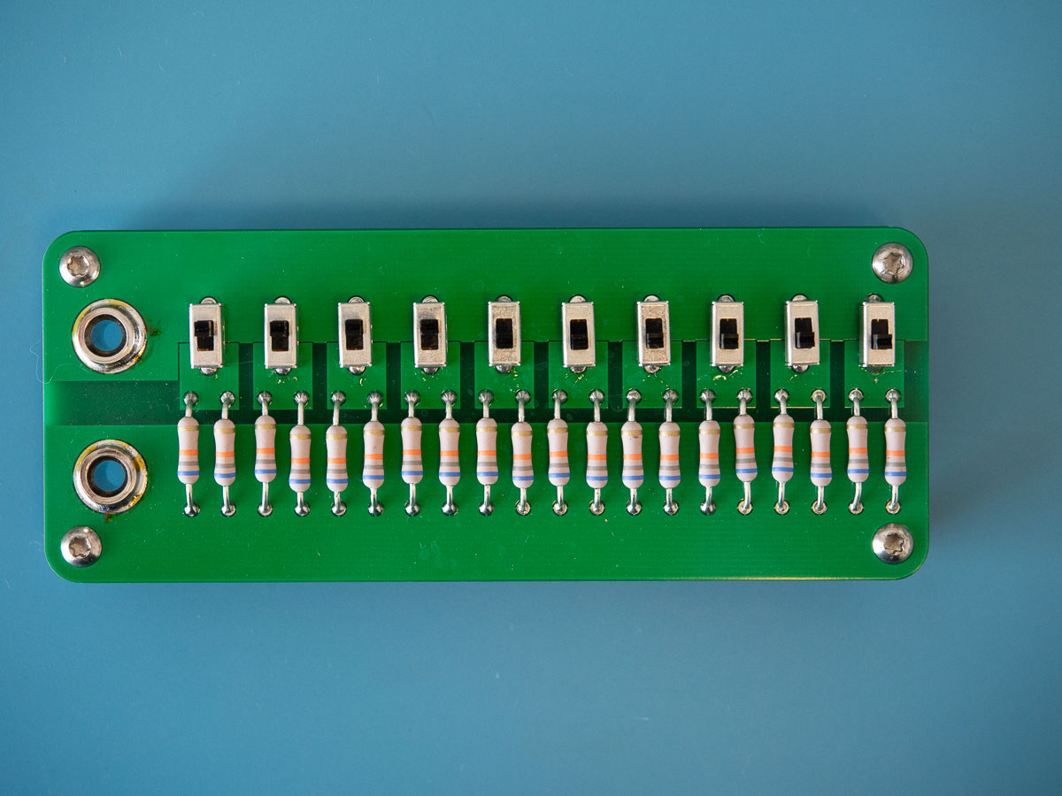
I don’t have an electronic load, so I also designed a simple circuit board with switches and resistors to step the load for faster, repeatable evaluation. Each switch on this board adds a branch with two 1 W 68 kΩ resistors in parallel, so the output current at 170 V can be adjusted from 0–50 mA in 5 mA steps. Using the switchable load board, I made efficiency measurements by recording source and load power levels while stepping the load. The converter is capable of 85–90% efficiency over a wide range of input voltage and output current.

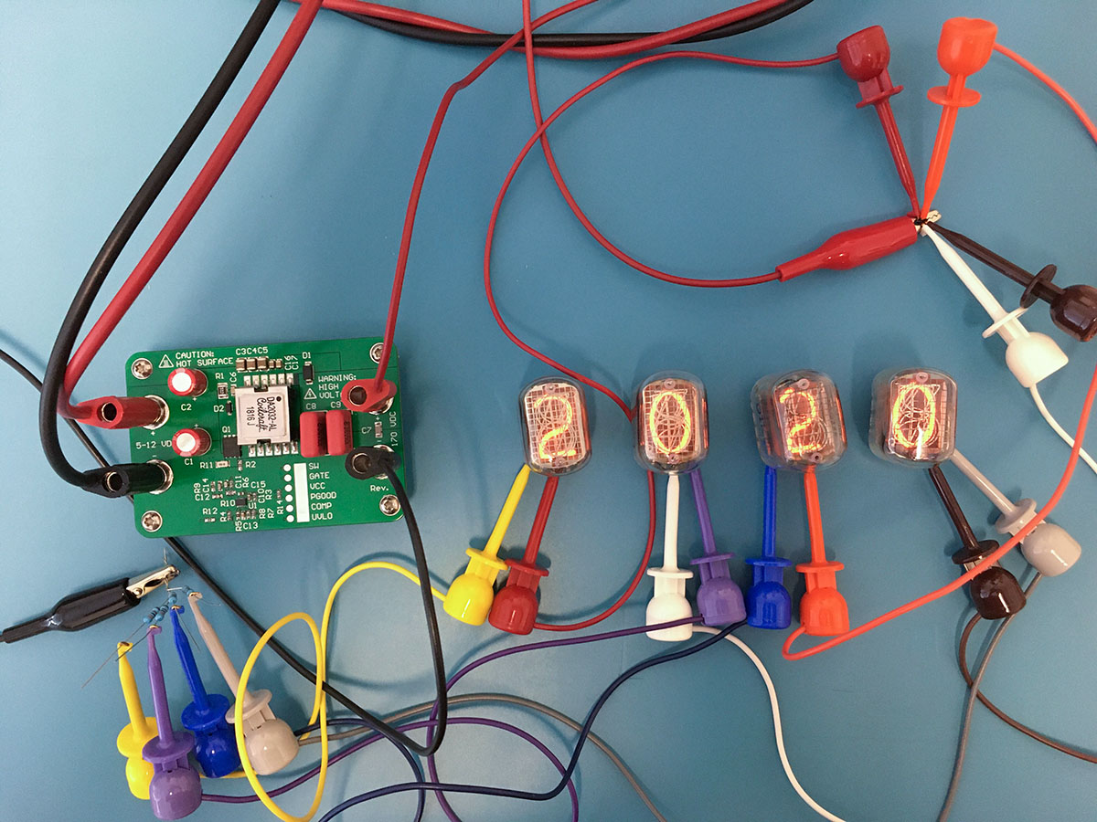
Finally, to show it actually lighting some Nixie tubes:
Further work
The flyback converter shows excellent performance and efficiency, but as an evaluation module, it’s not optimized for space, parts count, or cost. The design can likely be miniaturized with smaller component packages and other changes. If you have a Nixie tube project with special power needs, I would be interested to consult on your power design or integrating this converter into your project.
References
[1] R.W. Erickson and D. Maksimović, Fundamentals of Power Electronics, 3rd ed. Cham, Switzerland: Springer, 2020.
[2] Jian Sun, D. M. Mitchell, M. F. Greuel, P. T. Krein and R. M. Bass, “Averaged modeling of PWM converters operating in discontinuous conduction mode,” IEEE Transactions on Power Electronics, vol. 16, no. 4, pp. 482–492, July 2001, doi: 10.1109/63.931052.
[3] Texas Instruments, 2.2-MHz Wide Input Nonsynchronous Boost, SEPIC, Flyback Controller, LM5155 datasheet, Dec. 2018 (Revised Jan. 2021).
[4] Fairchild Semiconductor, Design Guidelines for RCD Snubber of Flyback, Application Note AN-4147, Jun. 2005.
[5] Texas Instruments, How to Measure the Loop Transfer Function of Power Supplies, Application Note AN-1889, Oct. 2008 (Revised Apr. 2013).
The schematics and PCB layout of the evaluation board, along with simulation and design scripts, are available on Github.
Original project logs for the design and evaluation of the converter are on hackaday.io.