Exploring power distribution networks
Anyone who has done electronics design knows the importance of bypass or decoupling capacitors, but mostly through received wisdom such as: “each IC should have a .1 µF capacitor,” “add one 1 µF for every eight ICs,” place decoupling capacitors “as close as possible,” and so on [1][2]. There’s very little in popular sources about experimentally measuring and verifying the effect of capacitor networks.
A circuit board typically receives power from a source off-board and then passes it through a voltage regulation module to provide a steady voltage to the rest of the board. A circuit board’s power distribution network (PDN) consists of everything between the voltage regulator and the power-consuming devices on the board, including bulk and decoupling capacitors, traces, and power planes and interconnecting vias. The purpose of the PDN is to deliver clean, low-noise voltage to the rest of the circuit board. Voltage noise on the PDN is the result of transient currents passing through the impedance of the PDN, and the goal in PDN design is to provide an acceptably low impedance from DC to the highest frequency of interest for the circuit.
The standard for measuring PDN impedance is a vector network analyzer (VNA) in a two-port shunt-thru connection [3]. VNAs are very expensive and most are designed for applications in radio and microwave communications rather than general impedance analysis (frequency ranges going up into the tens of gigahertz, but bottoming out at hundreds of kilohertz or the low single-digit megahertz range). I’ve been exploring using a more humble setup of a spectrum analyzer and tracking generator to get good results, as long as some reasonable assumptions hold.
The two-port shunt-thru measurement technique
In this measurement, an unknown impedance

The scattering parameters of this network are
If
The frequency range of the analyzer also places some limitations on the capacitance we can effectively measure. For the best results,
In the above circuit diagram, the ground terminals of the two ports are connected internally within the network analyzer. This ground loop creates a path for common-mode current that will distort measurements. Above 1 MHz, the inductance of this loop alone is typically enough to suppress common-mode current. For accuracy at lower frequencies, there are two standard methods to break the ground loop: use a common-mode choke, or a semi-floating differential amplifier. The latter provides better accuracy, but is an active device that would be another project to build or buy. A common-mode choke can be as simple as winding several turns of coaxial cable around a toroid core.
Test PCB
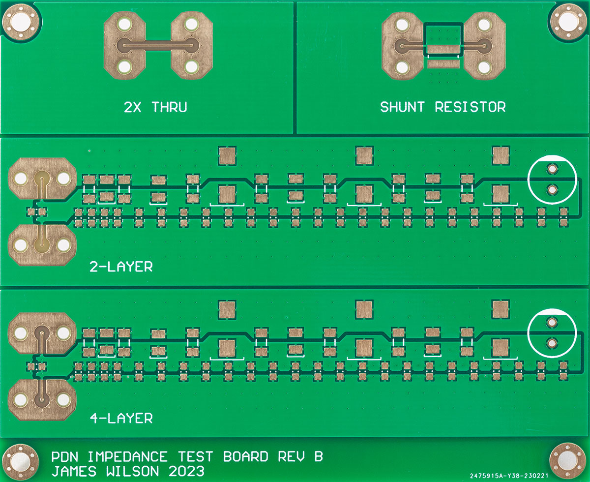
I designed a circuit board with the goal of being able to explore a wide variety of PDN phenomena [4]. I wanted a flexible test platform I could configure to emulate real PDNs by varying the number, position, and type of capacitors.
The requirements for my test PCB were:
- two closely-spaced coaxial ports for attachment of RF cables.
- footprints for decoupling and bulk capacitors of different type, and at varying distances. Ceramic, tantalum, and aluminum capacitors all have their own size categories. For simplicity, I used ceramic 0603 footprints for decoupling capacitor slots, and ceramic 1206, tantalum case codes A (1206) and D (2917), and 3.5mm-spacing radial aluminum capacitors.
- multiple test coupons: a two-layer stackup (power and ground on top, ground on bottom layer), a four-layer stackup (power and ground on top, ground on layer 2, power on layer 3, and ground on layer 4), one coupon for precision low-resistance measurement, and a 2x thru coupon for calibration
I used solderless compression-mount SMA connectors for the RF ports. These connectors are individually expensive, but reusable. I expected to use several boards in different configurations so reusable connectors had considerable cost savings. For the highest DC precision, I had the PCB made with 1 oz inner copper and 2 oz outer copper. ENIG finish ensured a flat surface for the compression-mount connectors.
Common-mode choke
As described earlier, the ground loop in the shunt-thru topology introduces measurement errors at low frequency. Introducing a common-mode choke in the measurement path suppresses the unwanted common-mode current and improves the accuracy of the measurement. The construction of my common-mode choke was a small project in its own. I chose a large nanocrystalline core (VAC T60006-L2090-W518) because this material is well-suited for a choke. Compared to ferrite, it is more broadband in its absorption range. Around this core, I wound hand-formable RG-402 cable. This cable is low-loss, thin but sturdy, and has a low bend radius for a compact final design. I also designed and 3D-printed a coil former to fit over the core [5]. The coil former supports the cable so it stays above its minimum bend radius and provides a guide for the split-winding design with a consistent number of turns around the core in both directions. I terminated the cable with BNC connectors and put the assembly into an enclosure for easy setup on the bench.

The performance of a choke can be evaluated by comparing its insertion loss in common mode and differential mode. The differential-mode measurement is as simple as connecting it to a network analyzer using cables. In common mode, either the shield or center conductor terminals of the choke are left unconnected, while the signal travels through only one of the conductors. For my test fixture, I connected the center conductors of a pair of coaxial pigtail probes to the outer shells of the choke’s BNC terminations. The pigtail shields were shorted together by touching them to the edge of a copper sheet placed under the choke’s enclosure. In the frequency range of interest below 1 MHz, the choke has neglible differential-mode insertion loss and between 20–50 dB of common-mode insertion loss. Differential-mode insertion loss remains below 2 dB across the FPC-1500’s measurement range. This compares well to a commercial common-mode choke for PDN testing.
Experiments
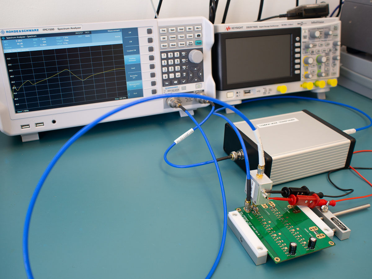
For my tests, I am using a Rohde & Schwartz FPC-1500 5 kHz – 3 GHz spectrum analyzer with tracking generator and a common-mode choke of my own design. Any similar spectrum analyzer with tracking generator, such as the Rigol DSA815-TG or Signal Hound SA44+TG44, will do. The nanoVNA can also be used with full vector measurement of
Decoupling capacitor placement
For the first experiment, I tried placing a single 100 nF capacitor at various distances from the measurement ports.
Design guidelines stress placing decoupling capacitors “as close as possible.” What does this really mean and how close is close enough? The reason that distance matters is not resistance, but inductance. Capacitors act like local power supplies on the board, supplying current to keep a steady voltage when there’s a surge in demand. Current flows in a loop from the capacitor, to a load, and then returns through ground. This current loop has inductance proportional to its area, so a closely-placed capacitor has a smaller loop and less inductance. Four-layer PCBs have a ground plane less than 1 mm (0.2 mm in this board’s stackup) underneath the top layer, so the return current couples tightly to the top layer and flows directly underneath it, further reducing the inductance.
For the experiment, I took measurements of the 100 nF capacitor placed between the measurement ports (as close as possible, or “ACAP”), and at distances of 10 mm and 98 mm, the farthest spot on the board. I repeated these measurements for the two-layer and four-layer sections of the board. By saving the spectrum analyzer data and applying the formulas to calculate the impedance, I got the following charts:


As a sanity check, most manufacturer characteristic charts for their 100 nF capacitors show they have their self-resonant frequency (SRF) between 20–30 MHz and have an ESR at this frequency of 20–50 mΩ. There’s a little bit of inductance from traces on the board to connect the ports, so overall this seems reasonable.
From the charts, it’s clear that capacitor placement matters much more on the two-layer board. Even 10 mm away, the frequency range where the capacitor impedance is less than 1 Ω has vastly shrunk. The four-layer board also shows this effect, but a .1 µF capacitor placed 10 mm away is nearly just as effective.
Bulk capacitor placement
Decoupling capacitors are supposed to be placed as close as possible, but guidelines are usually more lax for the placement of bulk capacitors. How does this advice fare against measurement?
For evaluating bulk capacitance, I used a 100 µF tantalum capacitor. My test board has three slots available for 2917 (case code D) tantalum capacitors at distances of roughly 32, 54, and 77 mm. Because this capacitor is active at frequencies near the low end of the FPC-1500’s range, I tried an indirect method of measurement: letting it resonate against a 100 nF capacitor, and measuring the resonant frequency at different mounting distances. The 100 nF capacitor is fixed in the ACAP slot. The resonant frequency will be the low MHz range, allowing for some better resolution on the spectrum analyzer. If mounting distance substantially affects the bulk capacitor, the resonant frequency should shift. Here is that result:


On the four-layer board, bulk capacitor distance has almost no effect on the PDN. Even on the two-layer board, the shift in resonant frequency is small compared to the previous experiment with a single 100 nF capacitor.
DC bias derating
A trap for new designers is the DC bias effect of class II ceramic capacitors (anything that is not C0G/NP0 temperature coefficient). When a DC voltage is applied to these capacitors, the effective capacitance is reduced in proportion to the voltage. Class II ceramics are popular because they provide capacitance up to about 10 µF in small packages. When used as decoupling capacitors they sit across the DC voltage rail, and their capacitance may need to be derated. This effect is easy to demonstrate using my test setup. To inject a DC voltage into the PDN, I used a bias tee connected to my bench power supply. The bias tee’s RF+DC port is connected to the test PCB, and the RF connection goes to the tracker generator output. Most spectrum analyzers, including the FPC-1500, have a DC blocking capacitor at the input, so no additional DC block is needed for the other port.
For this test, I mounted a 100 nF capacitor in the ACAP slot, and adjusted the DC bias voltage. This particular part is a 50 V X7R capacitor, which I use a lot because it is supposed to have negligible derating at 5 V.
This chart shows the impedance at frequency at different DC bias levels, as well as the calculated change in capacitance at 2 MHz. As described earlier, the calculated capacitance figures have a small error since the SA+TG setup can only measure the magnitude of impedance.

From the chart, it does appear the DC bias effect for this capacitor at 5 VDC is nothing concerning, but at 12 VDC and 24 VDC, it has become enough to consider derating.
Decade capacitors
Typically a designer combines bulk and smaller decoupling capacitors with the goal to create a PDN that is low-impedance across a wide frequency range. One rule-of-thumb suggestion that comes up is to combine capacitors from multiple decades (.1 µF + 1 µF + 10 µF + 100 µF) to cover all the bases. How well does this work? For this experiment, I set up the test board with a range of capacitors from 10 nF to 100 µF, with the smaller capacitors positioned closer to the ports. I used ceramic capacitors for 10 µF and below, and an aluminum electrolytic capacitor for the 100 µF part. I first measured each part individually in its chosen position. The following chart shows the individually measured capacitors, and then the parallel combination of all of them:


The careful eye will catch the 10 nF and 100 nF parts appear to have flat impedance at low frequencies. This is the approximation error mentioned earlier. Once the total impedance is more than a few ohms, scalar shunt-thru measurements show increasing error. In a passive network,
It appears the decade capacitor arrangement does work to create a wideband low-impedance PDN, with some pitfalls. To find the impedance of a parallel network, we generally trace along the minimum of the curves, and this mostly works here. There are several sharp peaks on the chart, caused by resonances between the capacitors. They are particularly bad in the two-layer board, and because ceramic capacitors have very low equivalent series resistance (ESR) that would otherwise dampen resonances. This is why ESR is a feature, not a bug, among some classes of capacitors. The ESR of many tantalum and aluminum capacitors help de-Q the network, increasing the bandwidth where the capacitor is at (relatively) low impedance and softening resonances.
Power plane capacitance and board resonance

The previous experiment showed some resonances in the UHF range, so I tried to see if they matched the expected power plane capacitance of the four-layer stackup. From the design files, the total area of the power and ground planes (layers 3 and 4) in the four-layer coupon is 2445 mm2. Additionally, there is a power pour on the top layer that couples to the ground plane below that measures about 400 mm2. Using the layer stackup data and the parallel plate capacitance formula
To check this prediction, I measured the board without any placed components. On the two-layer board, the interplane capacitance is too small to be measured, and can only be detected by the resonance near 400 MHz. On the four-layer board, the calculated interplane capacitance of 700 pF appears to match the observed result.

Precision low-value resistance measurements
With good equipment, the shunt-thru technique is capable of measuring impedances down into the single-digit milliohm range. I wanted to test the limits of my measurement setup by characterizing precision resistors below 10 mΩ. Measuring resistance this small is complicated by the need for careful fixture removal. The cables, connectors, and board traces all add losses that are comparable to a milliohm-range resistor, so the effect of these components has to be measured and removed before processing data.
The shunt resistor coupon on the test board has a footprint for a 1020 resistor. These wide-terminal resistors typically have lower equivalent series inductance (ESL), extending the range where they should show flat, resistive impedance. Nonetheless, even with ESL below 1 nH, a 1 mΩ resistor will become inductive below 1 MHz, so measurements need to be done at low frequency.
Fixture removal was done by first doing a response calibration using the 2x thru coupon, followed by de-embedding a short connection of the resistor pads. Only the short was de-embedded since it can be assumed that at low frequencies any parasitic admittances would be overwhelmed by the resistor under test. Furthermore, this de-embedding can be applied without a VNA under the earlier simplification that

I measured three resistors from the Vishay WSL series: 1 mΩ, 3 mΩ, and 5 mΩ. The 1 mΩ resistor shows a rising impedance over the measured range; this is consistent with its rated inductance just below 1 nH. The other impedance curves are mostly flat, which seems to indicate the de-embedding is correct. There is still about a 20% error in the magnitude that is unaccounted for that could be due to a poor response calibration.
Summary and future work
Even without a dedicated low-frequency VNA, it’s possible to obtain accurate measurements of PDNs with only a spectrum analyzer and tracking generator as long as the measured impedance is low, and we only need the magnitude of
The biggest obstacle for extending this work to in situ analysis of PCBs is the difficulty of probing. Even more miniature RF connectors take up too much space to be practical, and they can’t be placed everywhere of potential interest. Designing a well-characterized probe that can straddle a single surface-mount capacitor would be the next step in advancing this measurement technique for analyzing new and existing designs.
References
[1] P. Horowitz and W. Hill, The Art of Electronics, 3rd ed. New York: Cambridge University Press, 2015, pp. 856–857.
[2] P. Scherz and S. Monk, Practical Electronics for Inventors, 4th ed. New York: McGraw-Hill Education, 2016, pp. 343–347.
[3] I. Novak and J. Miller, Frequency-Domain Characterization of Power Distribution Networks. Norwood, MA: Artech House, 2007, pp. 126–129.
[4] Gerber manufacturing files for the test PCB
[5] Solidworks and STL design files for the coil former