2 GHz Active Probe
Students, hobbyists, and professionals today enjoy unprecedented access to powerful and affordable test equipment for understanding and building electronic projects. But as enthusiast projects have become more advanced and ambitious, it is still possible to hit the limits of entry-level equipment. I have been excited about open source hardware as an avenue to advance the performance and accessibility of test equipment, in much the same way the early open source software focused on development tools as a foundation for greater access to computing. This article is about my experiences building an open hardware single-ended active probe.
For most of us, our experience with oscilloscope probes begins and ends with passive probes. These appear at first to be a simple resistive divider with some capacitive compensation to extend their range, but hide a number of complex tricks. For one, it’s remarkable they work at all. Transmission line theory suggests connecting a device under test (DUT), which could have any source impedance, to a long transmission line that is terminated by an unmatched load (namely, the oscilloscope front end) is recipe for signal reflections. Yet in most cases, these probes work just fine without ringing or distortion. The trick, invented by Tektronix in the 1950s [1], is to use a lossy transmission line in the probe cable by replacing the inner conductor with resistance wire. This damps signal reflections, and together with carefully chosen compensation capacitors, yields a flat, wideband response.
These methods have their limits, which mean 10× passive probes can achieve a few hundred megahertz of bandwidth and have an input capacitance of 10–20 pF. Even at lower frequencies, this capacitance is sometimes high enough to make passive probes a poor choice. A crystal oscillator uses a load capacitance that is comparable to this number, so connecting a passive probe will immediately detune the circuit.
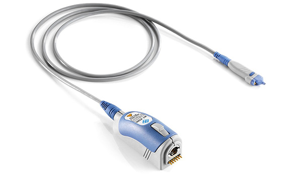
Active probes shine with high-frequency circuits or ones that require low loading, because their input capacitance is smaller by an order of magnitude. The operating principle behind an active probe is to use a buffer amplifier that has high input impedance and reproduces the signal at lower output impedance. The output impedance of the amplifier can be controlled to match the transmission line and oscilloscope termination for higher signal integrity. However, commercial active probes typically cost several thousand dollars. They take advantage of proprietary connectors that allow the probe to automatically configure the oscilloscope and use a single cable for power and signal, but this convenience locks you in to the vendor’s ecosystem. This usually doesn’t trouble professional labs that can afford to buy bundled packages of instruments and accessories, but it means even used active probes are often difficult for enthusiasts to work with.
DIY designs of active probes using discrete components have been done before, but they haven’t matched the bandwidth of commercial devices, and usually lacked the flexibility of DC coupling. The recently introduced BUF802 has made it possible to overcome these limitations and build very high performing analog front ends using off-the-shelf components and low-cost designs. The BUF802 is unity-gain buffer amplifier with a bandwidth of 3 GHz. A project is now underway to build an open source oscilloscope using this chip in the front end, and I’ve been experimenting with a complementary effort to build a single-ended active probe, with the following design goals:
- DC–2 GHz analog bandwidth, 10:1 attenuation
- Input impedance of 1 MΩ // 1 pF, 50 Ω output impedance
- Rated performance achievable on OSH Park FR-408HR four-layer stackup
- Minimum component size of 0402 and no BGA parts
- Open source design and repairable
Development history
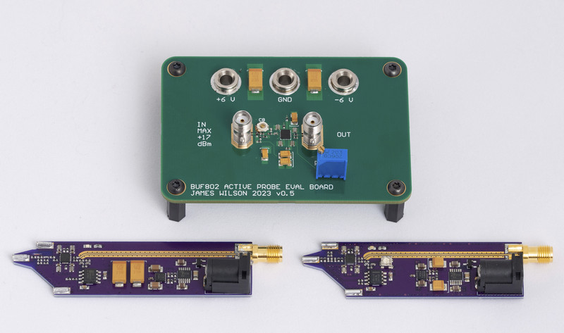
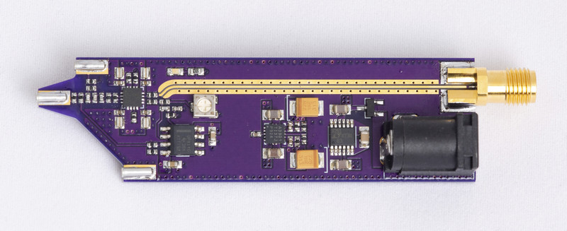
The BUF802 first came to my attention in late 2022 and I began researching how to use it as an active probe amplifier. I designed a non-form-factor evaluation board where the input and output were coupled to coaxial connectors for bench testing.
I designed and tested an initial rev A probe in late 2023 and found the location of the ground socket wasn’t optimal, and this was followed quickly by a rev B which incorporated a second ground socket without other changes. The rev B design was able to meet the 2 GHz bandwidth goal in testing. Since that time, I also obtained a Bode 100 VNA, which I used to examine the power distribution network and the crossover region performance. These measurements and further experiments showed the trimmable PCB capacitor used for frequency compensation was too lossy. Rev C incorporated minor optimization to PDN components and a redesign of the input network to use fixed frequency compensation capacitors, while making low-frequency attenuation trimmable.
The design files and this documentation are licensed under the terms of the CERN Open Hardware License (CERN-OHL-S version 2).
Design and simulation files on Github
Performance summary and methodology
The following charts show the performance of the rev C probe measured on a network analyzer. The probe shows a very flat response with a 3 dB bandwidth just over 2 GHz. The input impedance is about 1.1 pF, with with a


An alternative view of the input impedance is to look at return loss when the probe is used in a 50 Ω environment. Here the return loss of a 50 Ω terminated line is shown in a magnitude and Smith chart, with and without the probe attached. The return loss of the probed line remains better than 13 dB.


There is something of an industry schism on how to properly characterize the performance of high-frequency probes. This could be called the what-was vs. what-is controversy [2]: should a probe seek to accurately reconstruct the signal that was present before the probe was attached (what was), or should it seek to show the signal as it is loaded by the impedance of the probe (what is)? In an ideal world, the probe would have infinite impedance and these two positions would converge. When the probe has finite impedance, then the voltage at the probe input
Compounding this confusion is the reality that probes are used the field where conditions vary greatly. The nature of the connections from the probe sockets to the DUT greatly impact the parasitics and performance. The probe is usually held in hand, which challenges day-to-day and person-to-person consistency. To get any hope of consistent benchmarking, vendors measure probe performance using a fixture that minimizes variation and parasitics, as have I. In one of its application notes, Keysight freely admits this means “the probe’s specified bandwidth is [typically] unachievable in any everyday, usable configuration” [4]. Consequently, bandwidth charts for any probe should be considered as a best-case scenario.

The test fixture here is just a PCB with a 50 Ω exposed thru line and end-launch connectors. Characterizing the probe response is done with a two-port network analyzer. First, a response calibration is made with the analyzer ports connected via the thru fixture, and then the fixture’s port 2 connection is replaced with a termination. The probe output connects to port 2, making the transfer function

For measuring input impedance, the one-port measurement setup involves performing a calibration and then connecting the terminated thru fixture. The calibration plane is at the connector to the fixture, and the line must be probed as close to this point as possible. To squeeze a little more accuracy out of the calculation, I used the VNA to measure the electrical length from the calibration plane to the board/connector interface, and then added this as a port extension. This adjusts the calibration plane to almost exactly the point of contact with the probe. The return loss is measured with and without the probe connected, and then the probe input impedance can be backed out of these measurements by assuming the probe impedance is in parallel with the impedance of the terminated thru line.
Characterization of the probe in the crossover region started with a mystery and revealed some disappointing limits on the board stackup. In the frequency range of 10 kHz to 10 MHz, the probe output transitions from being driven by feedback from the precision amplifier to following the input resistive divider, and then the capactive divider. Ideally, the response should be flat. If the input network frequency compensation is imperfect, then one would expect to see flat regions at the low and high end, and a sloping transition between. Instead, I saw the following peaking response.


This behavior was puzzling because it didn’t appear in simulation, and also is less prominent with the evaluation board, which has only about 0.1–0.2 dB of peaking in this range when properly compensated. My first hypothesis was the combination of misadjusted frequency compensation and transmission line loss. The evaluation board provided a means to test the hypothesis: the frequency compensation capacitor is a trimmer for easy tuning, and I could interpose a length of poor cable and see if the result matched the chart. When I adjusted the frequency compensation and added a section of RG178 (a thin type of coaxial cable only suitable for short runs), the response demonstrated a similar peaking shape. Given the low frequency, the likely source of the cable loss is from conductor loss rather than dielectric loss.
(Update: June 2024) Mystery solved? Not quite. I made a test coupon of the output transmission line and measured it. Over the crossover region, it showed a mere 0.04 dB loss with increasing frequency, much less than the measured result. I turned my attention back to the input network. The design simulations did not account for parasitic capacitance in the high-valued resistors. In some cases, parasitics can be disregarded by accounting for them when chosing an explicit compensation capacitor. In other cases, particularly
To reduce the parasitic capacitance, an obvious move is to split a large resistor into a series combination. Diminishing returns set in quickly as other parasitics are introduced by increasing parts count. Some more testing is needed to see if this yields a practical improvement for the last 3–4% of flatness in this region.
Design overview

The active probe has three main components in this overview block diagram. An input network is responsible for passive attenuation and frequency compensation. The amplifier block contains the low- and high-frequency amplifiers that work together to provide a flat, wideband response, and an output matching network including the transmission line to the output connector. The power supply block uses a charge pump and dual low-dropout (LDO) voltage regulator to supply positive and negative DC voltage to the amplifier.
The BUF802 has has wide bandwidth but poor DC accuracy (typical input offset voltage of 600 mV), so the amplifier is structured as a composite loop where the signal is split by the input network and then re-combined inside the BUF802. DC and low frequencies are buffered by a low-offset op amp (OPA140), and high frequencies buffered by the BUF802’s JFET amplifier. For a while during the chip shortages of 2021–2023, the OPA140 was scarce, and I substituted the ADA4625 in early design experiments. Both of these amplifiers work well in this design, but the OPA140 is much cheaper. JFET op amps are preferred here because of their low input bias current, and noise and offset levels that compare well to bipolar amps. The board layout intentionally uses a larger SOIC-8 footprint for the op amp, since this is an industry-standard package for single-channel op amps that will permit part substitution.

In a conventional composite loop, the low- and high-frequency paths are combined with a resistor-capacitor network at the input node of the buffer. The BUF802 offers internal combination that provides better isolation between the signal paths [5]. Without the pole from the R-C network in its output path, the op amp’s phase margin and closed loop bandwidth are improved, and the crossover frequency shifts higher. Since this circuit isn’t exactly equivalent to the conventional composite loop, I’ve opted to show the BUF802 as a “two-input buffer” in the basic schematic.
In the input network, the tip resistor R1 sets the probe’s minimum input impedance and damps the resonance imposed by the probe’s input capacitance and the ground lead inductance. It is critical this resistor is placed as close as possible to the probe tip. An additional damping resistor R2 allows fine tuning of the probe’s bandwidth and peaking response. In the most recent board revision, I found this to have no benefit and fitted a jumper in its place, and I may remove it entirely from the design in the future.
The main signal path uses a frequency compensated voltage divider. Like in a passive probe, this circuit has useful properties: the transfer function is flat at all frequencies, and the capacitance of the BUF802 is isolated from the input in proportion to the divider attenuation. A 1.6 MΩ and 400 kΩ divider provides 5× attenuation, and another 2× comes from the doubly-terminated output to yield the target 10× attenuation. Increasing R3 to 422 kΩ compensates for the slightly less-than-unity gain of the BUF802 and improves crossover region flatness. The BUF802’s input capacitance is 2.4 pF, so the required compensation for a 5× divider is 2.4 pF / 4 = 0.6 pF. In the probe board, using two capacitors in series allows for easier tuning of the output level. I found a combination of 1.1 pF and 1.3 pF delivered almost exactly −20 dB at 100 MHz. Trimmer capacitors are also an option, but they are physically large and have worse parasitics. In earlier revisions, I used the PCB itself with a parallel-plate capacitor between layers 1 and 2 on the board. This amount of capacitance requires only a small area of copper, and the top layer can be trimmed off with a hobby knife to obtain the desired attenuation. However, I found this to be frustrating (once you remove copper, it’s gone!) and aspects of the probe’s performance demonstrated the PCB dielectric was much lossier than the datasheet led me to believe.
The signal path to the precision amplifier does not use compensation. A flat input characteristic is not needed here since this signal path is only used at low frequencies, and it is better to isolate as much of the op amp’s input capacitance as possible. The trace to get from the tip to the op amp is long enough to be considered a transmission line, so the probe board has a series termination resistor at the noninverting input (not shown). An R-C filter between the op amp and auxiliary input of the BUF802 attenuates signal and noise above the amplifier’s useful bandwidth. Circuit simulation shows the OPA140 runs out of closed-loop bandwidth around 30 kHz, so a 5.6 kΩ + 100 pF filter will set a corner frequency one decade higher.
The resistor values for the alpha and beta networks were chosen after some iterative trial and error subject to several constraints:
- The resistance looking into the alpha network needs to be 2 MΩ to make the parallel resistance of both signal paths equal to 1 MΩ.
- The gain of the the amplifier must match the main signal path gain of 1/5. The variable resistor
is realized with a 10 kΩ resistor in series with a 1 kΩ trimpot. - To compensate for the op amp’s input capacitance, a feedback capacitor is added to make the poles and zeros of the system gain cancel out; the required capacitance is given by
. - The input resistance of the beta network needs to be high enough not to disturb the 50 Ω output impedance.
should be placed as close as possible to the BUF802 output to prevent signal reflections.
In most high-frequency circuit design, the ground plane is your friend: it makes the impedance of traces well-defined and protects the circuit from both radiating and receiving noise. Here, it is not helpful because it adds shunt capacitance from the pads and traces of the input network, so the ground plane is voided underneath the components from the tip to the BUF802 input pin.
The power supply combines a LTC3261 charge pump to create a negative voltage rail, followed by a TPS7A39 dual positive and negative LDO. The BUF802’s bipolar output stage is quite thirsty and consumes nearly 40 mA of idle current, so some classic charge pump ICs like the 7660 are inadequate unless paralleled. The LTC3261 has a wider input voltage range, and can source 100 mA of current, making it a good single-chip solution.
A charge pump is a type of switching converter that uses only capacitors, and it tends to suffer from high output voltage ripple. The other board blocks need a high power supply rejection ratio (PSRR) to prevent the voltage ripple from coupling to the amplifier output. A back-of-the-envelope estimate for the peak-to-peak voltage ripple in the charge pump output is
Simulation
The use of simulation tools was critical to the design of the probe, and even then, I had to do multiple board spins to get things right. Circuit simulation (LTspice) was used to design the precision amplifier loop, both in selecting input network components and doing stability analysis of the loop. LTspice’s capability to simulate arbitrary Laplace transfer functions was also useful in testing my hypothesis around PCB dielectric loss.

The input network parasitics are particularly difficult to think about without simulation; there is no ground plane, and a lot of irregular geometry that will vary in real use. To characterize this transmission line based on physical geometry, a field solver is needed, and openEMS is one of the few free and open source solvers available. The openEMS simulation output is a Touchstone file, which is then converted to a SPICE subcircuit using s2spice. This can used in a SPICE simulation as a “black box” component replacing the input network. After testing many candidate layouts for the input network in openEMS, I was more confident the design could achieve the goals for input capacitance. The simulated and measured input capacitance show reasonable agreement, with differences attributable to simplistic modeling of the ground lead inductance.
openEMS was also used to match the output transmission line. OSH Park doesn’t offer a controlled impedance service, so you’re on your own for choosing a trace width to get a 50 Ω line. The trace thickness (1.7 mil) is significant compared to the dielectric (8 mil), and a field solver produces more accurate results than simple calculators when combining thick metal and coplanar waveguide lines. Tuning microstrip and coplanar waveguide lines is a great introduction to openEMS since the geometry is easy to express in code, and it’s very reuseable between projects.
References
[1] J. R. Kobbe and W. J. Polits. “Electrical probe,” U.S. Patent 2883619.
[2] Agilent Technologies. Side-by-Side Comparison of Agilent and Tektronix Probing Measurements on High-Speed Signals, Application Note 1491, January 2007.
[3] Tektronix. Probe Bandwidth Calculations, Technical Brief 60W-18324-0, November 2004.
[4] Keysight Technologies. Improving Usability and Performance in High-Bandwidth Active Oscilloscope Probes, Application Note 5988-8005, July 2014.
[5] Texas Instruments, Achieving high-DC Precision and Wide Large Signal Bandwidth with Hi-Z Buffers, Technical Article SSZT102, Jan. 2022.